Authors: jon stokes
Tags: #Computers, #Systems Architecture, #General, #Microprocessors
Inside the Machine: An Illustrated Introduction to Microprocessors and Computer Architecture (94 page)

aging, high-clockspeed Netburst microarchitecture that was currently at the
heart of the company’s desktop and server offerings. This being the case,
Intel’s Israeli team began working on an improved version of the Pentium M
that was intended for use outside the mobile market.
246
Chapter 12
Core Duo/Solo
The successor to the Pentium M (almost as widely known in computing
circles by its code name,
Yonah
, as by its official name,
Core Duo/Solo)
builds on the Pentium M’s microarchitecture and brings it to new levels of performance and power efficiency (see Table 12-2). However, Core Duo is
mainly an evolutionary, transitional design that sits between the Pentium M
and the more radically improved Core 2 Duo described in the next major
section of this chapter. This section will briefly cover the major ways that
Core Duo improves on the Pentium M before moving on to the next
section’s more detailed coverage of Core 2 Duo.
Table 12-2:
Features of the Core Solo/Duo
Introduction Date
January 5, 2006
Process
65 nanometer
Transistor Count
151 million
Clock Speed at Introduction
1.66 to 2.33 GHz
L1 Cache Size
32KB instruction, 32KB data
L2 Cache Size (on-die)
2MB
x
86 ISA Extensions
SSE3
Intel’s Line Goes Multi-Core
The Intel microarchitectures covered in previous chapters, especially the
Pentium 4’s Netburst microarchitecture, were designed so that their perform-
ance scaled primarily with clockspeed increases. But as you learned in the
earlier section on power density, the viability of this approach has been
rapidly diminishing in conjunction with shrinking transistor sizes. Instead
of trying to run a single narrow instruction stream faster by increasing the
processor’s clockspeed,
multi-core processors
like Core Duo are designed to exploit Moore’s Curves by integrating multiple copies of a microarchitecture
onto a single piece of silicon in order to execute multiple instruction streams
in parallel.
Processor Organization and Core Microarchitecture
Thus far, the discussions of microprocessor organization in this book have
placed all of a processor’s different components into a few basic categories.
My descriptions and illustrations depict processors as being divided primarily
into a front end and a back end, with each of these two main divisions consist-
ing of various high-level functional blocks (decode unit, branch-prediction
unit, integer unit, load-store unit, etc.), which are themselves made up of
more specialized units (simple/fast decoders, complex integer execution
unit, floating-point ALU, store-address unit, etc.).
Intel’s Pentium M, Core Duo, and Core 2 Duo
247
All of these different levels of organization come together to comprise a
processor’s
core microarchitecture
, or simply
core
, for short. Note that a processor’s core is typically understood to include the L1 cache, as well. Thus you’ll often encounter references in computing literature to the
P6 core
, the
Netburst core
, the
Pentium core
, and so on, all of which are short-hand ways of referring to a particular combination of L1 cache, front-end, and back-end hardware as
distinct from the other components on the processor die (for example, the
L2 cache or less commonly integrated components like an L3 cache or a
memory controller).
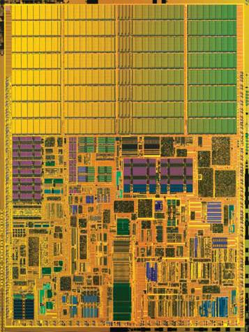
Figure 12-6 shows the floor plan of an Intel Pentium M processor. This is
a picture of the actual processor die, with the core microarchitecture marked
and distinguished from the L2 cache.
L2 Cache
Core
Figure 12-6: The floor plan of an Intel Pentium M processor
NOTE
The common use of the term core almost certainly explains Intel’s decision to use the
name Core in the branding of its new microarchitectures and their implementations.
Often, it’s also useful to draw a distinction between a microarchitecture—
conceived more abstractly as a particular arrangement of front end and back
end hardware—and one or more specific
implementations
of that microarchitecture. These implementations take the form of distinct microprocessor
products that are either based on the same microarchitecture (as in the
case of the Core 2 Duo E6300 [2MB of L2 cache] and Core 2 Extreme X6800
[4MB of L2 cache], both of which implement the Intel Core microarchitec-
ture) or on closely related microarchitectures that can be grouped together
into the same family (for example, the original Pentium 4 and the Pentium 4
with HyperThreading, both of which implement variants of the Netburst
microarchitecture).
248
Chapter 12
Multiprocessing and Chip Multiprocessing
For years, server, workstation, and even some consumer computers have
used a technique called
multiprocessing
to increase the amount of execution hardware available to operating systems and applications. In a nutshell,
multiprocessing is simply the integration of more than one processor core
into a single computer system. In a traditional multiprocessor system, separate
processor cores are implemented on separate pieces of silicon and are
packaged as separate integrated circuits, as shown in Figure 12-7.
Figure 12-7: A multiprocessor computer
However, the semiconductor industry has now moved to a technique
called
chip multiprocessing (CMP)
, where two or more processor cores are integrated onto the same silicon die. Under the CMP paradigm, the term
microprocessor
now refers to an integrated circuit that implements multiple copies of a core architecture on a single silicon die. Figure 12-8 is an abstract representation of a CMP computer containing what is commonly called a
dual-core processor
, a processor with two cores on the same die.
Different kinds of multi-core processors are often distinguished by their
levels of integration. Some multi-core processors, like Intel’s Netburst-based
Pentium D, have cores that share only a silicon substrate—each core has a
private L2 cache, and all inter-core communication buses are off-die. At the
other end of the spectrum is a more highly integrated multi-core processor
like the Core Duo, shown in Figure 12-9.
The two cores that make up the Core Duo each have a private L1 cache,
but they share an L2 cache. The Core Duo also includes some arbitration
logic that helps control access to the shared L2, so that neither core is able
to soak up all the L2 bus bandwidth for itself.
Intel’s Pentium M, Core Duo, and Core 2 Duo
249
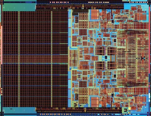
Figure 12-8: A chip multiprocessing (CMP) computer
NOTE
The dual-core processors in the Intel Core Duo/Solo line are named Core Duo, while
their smaller, cheaper, less powerful single-core counterparts are named Core Solo.
The shared L2 offers a number of advantages, not the least of which is an
increase in the ability of the two cores to share data without using a bus. If
both cores are using the same working set of code and/or data, then that
working set can be placed in the shared L2 where the cores can easily access
it simultaneously. Core Duo’s shared L2 also saves power, because both cores
use a single, shared bus to access it.
Core 1
L2 Cache
Core 2
Figure 12-9: The floor plan of an Intel Core Duo processor
250
Chapter 12
Core Duo’s Improvements
Core Duo’s architects took the basic microarchitecture of the second version
of the Pentium M, codenamed
Dothan
, and made a number of improvements
aimed at bringing the design to higher levels of performance and power
efficiency. These improvements are described briefly in the sections here.
Micro-ops Fusion of SSE and SSE2 store and load-op Instructions
On the Pentium M, only
x
86 and
x
87 load-op and store instructions can be micro-fused. All SSE and SSE2 load-op and store instructions must therefore
pass through the Pentium M’s single complex/slow decoder, a situation that
creates a serious bottleneck for 128-bit vector code with lots of memory traffic.
Intel fixed this bottleneck for Core Duo by enabling all three of the new
processor’s decoders to generate fused micro-ops for SSE and SSE2 load-op
and store instructions. Thus Core Duo’s decode phase can send up to three
fused 128-bit load-op and/or store micro-ops per cycle into the micro-op
queue. Because vector code is typically memory-intensive, Core Duo’s ability
to use any of its three decoders to process vector memory instructions is
critical to the design’s improved vector performance.
Micro-ops Fusion and Lamination of SSE and SSE2 Arithmetic Instructions
Even more significant for Core Duo’s vector performance than micro-fused
memory accesses is the fact that Core Duo also expands the use of micro-ops
fusion to encompass 128-bit vector arithmetic instructions. For reasons that
I’ll explain in this chapter’s discussion of Core 2 Duo, most SSE and SSE2
instructions decode into multiple micro-ops (typically from two to four) on
the Pentium III, Pentium 4, Pentium M, and Core Duo. This means that SSE
and SSE2 vector instructions have been bottlenecked at the decode phase on
processors prior to Core Duo because they can only be decoded by the slow/
complex decoder.
On Core Duo, 128-bit SSE and SSE2 vector instructions that decode into
a pair of 64-bit micro-ops can be translated into a single fused micro-op by all three of the front end’s decoders. Furthermore, vector instructions that
decode into two micro-op pairs (for a total of four micro-ops per instruction)
can be translated by the decoders into a single laminated micro-op. This
laminated micro-op
functions like a normal fused micro-op—it breaks apart into its four constituent micro-ops during the execute phase, but it’s tracked
and committed using a single ROB entry.
Core Duo’s ability to generate fused and laminated micro-ops for SSE
and SSE2 instructions is a crucial part of its superior vector performance.
Not only do lamination and the extension of micro-ops fusion to the SSE
family of instructions improve performance by eliminating a decode bottle-
neck, but these techniques also add to the design’s power efficiency by
enabling it to track more micro-ops using a smaller instruction window.
Intel’s Pentium M, Core Duo, and Core 2 Duo
251
Micro-ops Fusion of Miscellaneous Non-SSE Instructions
Core Duo also supports micro-ops fusion of a few new types of instructions
that had been forced to use the complex/slow decoder in previous designs.
These new instruction types include indirect branch instructions, compare/
test immediate and memory instructions, and some store immediate to
memory instructions. Finally, a handful of other multi-micro-op instructions
had the number of micro-ops into which they decode reduced, freeing up
dispatch, issue, and retire bandwidth.
Improved Loop Detector
One of the problems with the Pentium M’s loop detector is that it fails to