Make: Electronics (24 page)
Authors: Charles Platt

Essentials
All about NPN and PNP transistors (continued)
All-transistor basics
- Never apply a power supply directly across a transistor. You can burn it out with too much current.
- Protect a transistor with a resistor, in the same way you would protect an LED.
- Avoid reversing the connection of a transistor between positive and negative voltages.
- Sometimes an NPN transistor is more convenient in a circuit; sometimes a PNP happens to fit more easily. They both function as switches and amplifiers, the only difference being that you apply a relatively positive voltage to the base of an NPN transistor, and a relatively negative voltage to the base of a PNP transistor.
- PNP transistors are used relatively seldom, mainly because they were more difficult to manufacture in the early days of semiconductors. People got into the habit of designing circuits around NPN transistors.
- Remember that bipolar transistors amplify current, not voltage. A small fluctuation of current through the base enables a large change in current between emitter and collector.
- Schematics sometimes show transistors with circles around them, and sometimes don’t. In this book, I’ll use circles to draw attention to them. See Figures 2-91 and 2-92.
- Schematics may show the emitter at the top and the collector at the bottom, or vice versa. The base may be on the left, or on the right, depending on what was most convenient for the person drawing the schematic. Be careful to look carefully at the arrow in the transistor to see which way up it is, and whether it is NPN or PNP. You can damage a transistor by connecting it incorrectly.
- Transistors come in various different sizes and configurations. In many of them, there is no way to tell which wires connect to the emitter, the collector, or the base, and some transistors have no part numbers on them. Before you throw away the packaging that came with a transistor, check to see whether it identifies the terminals.
- If you forget which wire is which, some multimeters have a function that will identify emitter, collector, and base for you. Check your multimeter instruction booklet for more details.
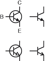
Figure 2-91.
The symbol for an NPN transistor always has an arrow pointing from its base to its emitter. Some people include a circle around the transistor; others don’t bother. The style of the arrow may vary. But the meaning is always the same. The top-left version is the one I use in this book.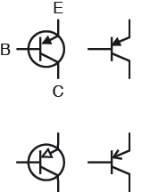
Figure 2-92.
The symbol for a PNP transistor always has an arrow pointing from its emitter to its base. Some people include a circle around the transistor; others don’t bother. The style of the arrow may vary. But the meaning is always the same. The top-left version is the one I use in this book.
Background
Transistor origins
Though some historians trace the origins of the transistor back to the invention of diodes (which allow electricity to flow in one direction while preventing reversal of the flow), there’s no dispute that the first working transistor was developed at Bell Laboratories in 1948 by John Bardeen, William Shockley, and Walter Brattain (Figure 2-93).
Shockley was the leader of the team, who had the foresight to see how potentially important a solid-state switch could be. Bardeen was the theorist, and Brattain actually made it work. This was a hugely productive collaboration—until it succeeded. At that point, Shockley started maneuvering to have the transistor patented exclusively under his own name. When he notified his collaborators, they were—naturally—unhappy about this idea.
A widely circulated publicity photograph didn’t help, in that it showed Shockley sitting at the center in front of a microscope, as if he had done the hands-on work, while the other two stood behind him, implying that they had played a lesser role. In fact Shockley, as the supervisor, was seldom present in the laboratory where the real work was done.
The productive collaboration quickly disintegrated. Brattain asked to be transferred to a different lab at AT&T. Bardeen moved to the University of Illinois to pursue theoretical physics. Shockley eventually left Bell Labs and founded Shockley Semiconductor in what was later to become Silicon Valley, but his ambitions outstripped the capabilities of the technology of his time. His company never manufactured a profitable product.
Eight of Shockley’s coworkers in his company eventually betrayed him by quitting and establishing their own business, Fairchild Semiconductor, which became hugely successful as a manufacturer of transistors and, later, integrated circuit chips.

Figure 2-93.
Photographs provided by the Nobel Foundation show, left to right, John Bardeen, William Shockley, and Walter Brattain. For their collaboration in development of the world’s first working transistor in 1948, they shared a Nobel prize in 1956.
Essentials
Transistors and relays
One limitation of NPN and PNP transistors is that they are naturally “off” until you turn them “on.” They behave like a normally open pushbutton, which conducts electricity only for as long as you hold it down. They don’t normally behave like a normal on switch, which stays on until you apply a signal to turn it off.
A relay offers more switching options. It can be normally open, normally closed, or it can contain a double-throw switch, which gives you a choice of two “on” positions. It can also contain a double-pole switch, which makes (or breaks) two entirely separate connections when you energize it. Single-transistor devices cannot provide the double-throw or double-pole features, although you can design more complex circuits that emulate this behavior.
Here’s a list of transistor and relay characteristics.
Transistor | Relay | |
Long-term reliability | Excellent | Limited |
Configurable for DP and DT switching | No | Yes |
Ability to switch large currents | Limited | Good |
Able to switch alternating current (AC) | Usually not | Yes |
Can be triggered by alternating current (AC) | Usually not | Optional |
Suitability for miniaturization | Excellent | Very limited |
Sensitive to heat | High | Moderate |
Ability to switch at high speed | Excellent | Limited |
Price advantage for low-voltage low-current | Yes | No |
Price advantage for high-voltage high-current | No | Yes |
Current leakage when “off” | Yes | No |
The choice between relays or transistors will depend on each particular application.
Theory
See the current
If you want to get a more precise understanding of how a transistor works, you should try this little test. It shows the precise behavior and limits of the 2N2222 transistor that you used in the previous experiment.
I’ve said that in an NPN transistor, the collector should always be more positive than the emitter and that the base should have a potential somewhere between those two voltages. Figure 2-94 shows this rather vague relationship. Now I want to substitute some numbers for these general statements.
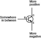
Figure 2-94.
The proper functioning of an NPN transistor requires you to maintain these voltage relationships.
Take a look at the schematic in Figure 2-95, and check the component values. Notice that the total resistance above the transistor, from R1 + R2, is the same as the total resistance below it, from R3 + R4. Therefore the potential on the base of the transistor should be halfway between the two extremes—until you use potentiometer P1 to adjust the voltage of the base of the transistor up and down.
The two 180Ω resistors, R1 and R3, protect the transistor from passing excessive current. The two 10K resistors, R2 and R4, protect the base when the potentiometer is turned all the way up or all the way down.
I would like you to see what the transistor is doing by measuring the amperage flowing into the base at the position marked A1, and the total amperage flowing out through the emitter at the position marked A2. To do this, it would be really helpful if you had two meters. As that may be impractical, the breadboard diagrams in Figures 2-96 and 2-97 show how you can swap one meter between the two locations.
Remember that to measure milliamps, you have to pass electricity through the meter. This means that the meter must be inserted into the circuit, and whenever you remove the meter, you have to remake the connection where the meter was. The breadboard diagram shows how you can do this. Fortunately, it’s very easy to remove and replace wires in a breadboard. Where wires are connected to the potentiometer, you may need to revert to using alligator clips.
Begin with the potentiometer turned about halfway through its range. Measure at A1 and A2. Turn the potentiometer up a bit, and measure current at the two locations again. Following is a table showing some actual readings I obtained at those two locations, using two digital meters simultaneously.
Milliamps passing through location A1 | Milliamps passing through location A2 |
0.01 | 1.9 |
0.02 | 4.9 |
0.03 | 7.1 |
0.04 | 9.9 |
0.05 | 12.9 |
0.06 | 15.5 |
0.07 | 17.9 |
0.08 | 19.8 |
0.09 | 22.1 |
0.10 | 24.9 |
0.11 | 26.0 |
0.12 | 28.3 |
There’s a very obvious relationship. The current emerging from the emitter of the transistor, through location A2, is about 240 times the current passing through location A1, into the base. The ratio of current coming out from the emitter of an NPN transistor to current going into the base is known as the
beta value
for a transistor. The beta value expresses the transistor’s amplifying power.
It’s a very constant ratio, until you push it a little too far. Above 0.12 mA, this particular transistor becomes “saturated,” meaning that its internal resistance cannot go any lower.