Make: Electronics (53 page)
Authors: Charles Platt

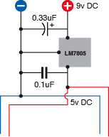
Figure 4-44.
This simple circuit is essential to provide a regulated 5V DC supply for logic chips.
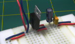
Figure 4-45.
The voltage regulator and its two capacitors can fit snugly at the top of a breadboard. Remember to apply the 9V input voltage at the left pin of the regulator, and distribute the 5V output down the sides of the breadboard.
After installing your regulator, take a couple of tactile switches, two 10K resistors, a low-current LED, and a 1K resistor, and set them around a 74HC00 logic chip as shown in Figure 4-46. You may notice that many of the pins of the chip are shorted together and connected to the negative side of the power supply. I’ll explain that in a moment.
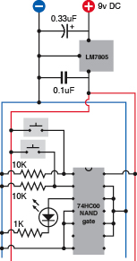
Figure 4-46.
By observing the LED when you press either, both, or neither of the buttons, you can easily figure out the logical function of the NAND gate.
Fundamentals
Voltage regulators
The simplest versions of these little semiconductors accept a higher DC voltage on one pin and deliver a lower DC voltage on another pin, with a third pin (usually in the middle) serving as a common negative, or ground. You should also attach a couple of capacitors to smooth the current, as shown in Figure 4-46.
Typically you can put a 7.5-volt or 9-volt supply on the “input” side of a 5-volt regulator, and draw a precise 5 volts from the “output” side. If you’re wondering where the extra voltage goes, the answer is, the regulator turns the electricity into heat. For this reason, small regulators (such as the one in Figure 4-8) often have a metal back with a hole in the top. Its purpose is to radiate heat, which it will do more effectively if you bolt it to a piece of aluminum, since aluminum conducts heat very effectively. The aluminum is known as a heat sink, and you can buy fancy ones that have multiple cooling fins.
For our purposes, we won’t be drawing enough current to require a heat sink.
When you connect power, the LED should light up. Press one of the tactile switches, and the LED remains illuminated. Press the other tactile switch, and again the LED stays on. Now press both switches, and the light should go out.
Pins 1 and 2 are logic inputs for the 74HC00 chip. Initially they were held at negative voltage, being connected to the negative side of the power supply through 10K resistors. But each pushbutton overrides its pull-down resistor and forces the input pin to go positive.
The logic output from the chip, as you saw, is normally positive—but
not
if the first input
and
the second input are positive. Because the chip does a “Not AND” operation, it’s known as a NAND logic gate. You can see the breadboard layout in Figure 4-47. Figure 4-48 is a simplified version of the circuit. The U-shaped thing with a circle at the bottom is the logic symbol for a NAND gate. No power supply is shown for it, but in fact all logic chips require a power supply, which enables them to put out more current than they take in. Anytime you see a symbol for a logic chip, try to remember that it has to have power to function.
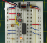
Figure 4-47.
This breadboard layout is exactly equivalent to the schematic in Figure 4-46.

Figure 4-48.
The structure and function of the NAND gate is easier to visualize with this simplified schematic that omits the power supply for the chip and doesn’t attempt to place the wires to fit a breadboard layout.
The 74HC00 actually contains four NAND gates, each with two logical inputs and one output. They are arrayed as shown in Figure 4-49. Because only one gate was needed for the simple test, the input pins of the unused gates were shorted to the negative side of the power supply.
Pin 14 supplies positive power for the chip; pin 7 is its ground pin. Almost all the 7400 family of logic chips use the same pins for positive and negative power, so you can swap them easily.
In fact, let’s do that right now. First, disconnect the power. Carefully pull out the 74HC00 and put it away with its legs embedded in conductive foam. Substitute a 74HC08 chip, which is an AND chip. Make sure you have it the right way up, with its notch at the top. Reconnect the power and use the pushbuttons as you did before. This time, you should find that the LED comes on if the first input AND the second input are both positive, but it remains dark otherwise. Thus, the AND chip functions exactly opposite to the NAND chip. Its pinouts are shown in Figure 4-50.
You may be wondering why these things are useful. Soon you’ll see that we can put logic gates together to do things such as create an electronic combination lock, or a pair of electronic dice, or a computerized version of a TV quiz show where users compete to answer a question. And if you were really insanely ambitious, you could build an entire computer out of logic gates.

Figure 4-49.
The pinouts of the logic gates in a 74HC00chip.
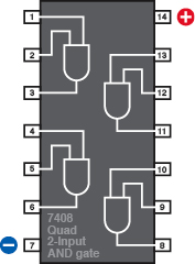
Figure 4-50.
The pinouts of the logic gates in a 74HC08chip.
Background
From Boole to Shannon
George Boole was a British mathematician, born in 1815, who did something that few people are ever lucky enough or smart enough to do: he invented an entirely new branch of mathematics.
Interestingly, it was not based on numbers. Boole had a relentlessly logical mind, and he wanted to reduce the world to a series of true-or-false statements which could overlap in interesting ways. For instance, suppose there is a couple named Ann and Bob who have so little money, they only own one hat. Clearly, if you happen to run into Ann and Bob walking down the street, there are four possibilities: neither of them may be wearing a hat, Ann may be wearing it, or Bob may be wearing it, but they cannot both be wearing it.
The diagram in Figure 4-51 illustrates this. All the states are possible except the one where the circles overlap. (This is known as a Venn diagram. I leave it to you to search for this term if it interests you and you’d like to learn more.) Boole took this concept much further, and showed how to create and simplify extremely complex arrays of logic.
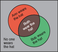
Figure 4-51.
This slightly frivolous Venn diagram illustrates the various possibilities for two people, Ann and Bob, who own only one hat.
Another way to summarize the hat-wearing situation is to make the “truth table” shown in Figure 4-52. The rightmost column shows whether each combination of propositions can be true. Now check the table in Figure 4-53. It’s the same table but uses different labels, which describe the pattern you have seen while using the NAND gate.
Boole published his treatise on logic in 1854, long before it could be applied to electrical or electronic devices. In fact, during his lifetime, his work seemed to have no practical applications at all. But a man named Claude Shannon encountered Boolean logic while studying at MIT in the 1930s, and in 1938 he published a paper describing how Boolean analysis could be applied to circuits using relays. This had immediate practical applications, as telephone networks were growing rapidly, creating complicated switching problems.